
Post 1: Designing a UART based communication system
Published:
Written by Shreya Datir, in collaboration with Muhammad Farhan Azmine
1. Introduction
The Universal Asynchronous Receiver/Transmitter (UART) is a simple yet powerful serial communication protocol that has been around for decades. It enables point-to-point data transfer using just two main lines, transmit (TX) and receive (RX). It is asynchronous, meaning that it doesn’t have a shared clock signal. It still continues to be widely used in microcontrollers, FPGAs, industrial equipment, despite the emergence of faster and more complex protocols like SPI, or I2C, because of its simplicity, low hardware requirements, and proven reliability.
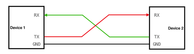
Photo from here
The image above shows a UART communication setup between two devices. In a real-world scenario, Device 1 could be a PC, microcontroller or another FPGA sending data to Device 2, which processes the data and sends a response back. In this project, we are only designing UART logic for Device 2. Device 1 will not be implemented on hardware, instead its behavior will be generated from a testbench in simulation. The testbench will send bytes of data to Device 2. Device 2 will accept the data and send back the processed data to the testbench. In this post, we will see how the UART logic can be designed using a simple finite-state machine (FSM). The data transmission follows a well-defined sequence: waiting in the idle state, detecting a start bit, shifting in or out data bits, verifying the stop bit, and returning to idle. By defining each state and its transitions clearly, an FSM ensures predictable timing, clean phase changes, and the ability to handle error conditions like invalid start bits or framing errors in a structured manner.
This post will begin by explaining UART signaling and timing fundamentals. It will then detail the design of both transmit (TX) and receive (RX) logic using FSMs, including the step-by-step state diagrams. Finally, it will show how to integrate these into a top-level module, test the design in simulation, and discuss considerations for implementing it on hardware.
2. Background: UART Essentials
UART communication is asynchronous, meaning the device 1 transmitter and the device 2 receiver do not share a common clock signal. Each of them operates on their separate clock and both ends agree beforehand on a baud rate which is the number of bits sent per second. Data is sent in a frame that starts with a start bit (logic low), followed by a fixed number of data bits (usually 8 and LSB first), an optional parity bit for error checking, and a stop bit (logic high) to signal the end of the frame. This structure allows UART to transfer data reliably over just two wires.
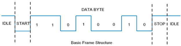
Photo from here
Baud rate generation and clock-to-bit timing
The baud rate is simply the number of signal changes (symbols) transmitted per second. In UART, one symbol corresponds to one bit, so the baud rate directly equals the number of bits sent per second. Since UART does not send a clock signal, each side must generate its own timing internally. A baud rate generator in the hardware divides the system clock to produce a timing reference that matches the agreed baud rate.
\[\text{Bit Period (seconds)} = \frac{1}{\text{baud rate}}\]For example, at 9600 baud, each bit period is ~104 µs long.
In RTL design, we work with Clock Cycles instead of time. To calculate the number of clock cycles in one bit period, we use the equation below:
For example, with a 100 MHz system clock and 115200 baud, the clock cycles per bit are 868. This means the UART logic must hold each bit steady for 868 clock cycles before moving to the next one. On the receive side, sampling is done at the midpoint of this window.
Common pitfalls (sampling errors, metastability)
While UART is straightforward, certain issues can degrade communication quality. Sampling errors occur if the receiver samples too early or too late within a bit period, leading to incorrect data. Metastability can happen when an asynchronous signal is read too close to a clock edge, causing unpredictable logic levels. Designers typically use oversampling and synchronizer flip-flops to minimize these risks and ensure stable, reliable data capture.
3. Designing the RX (Receive) FSM
The purpose of the RX FSM is to reconstruct a byte of data from the serialized bits sent through the single RX line. The UART receiver watches the line for a falling edge that marks a start bit, then waits half a bit period to sample in the middle-where the signal is most stable. From there, it samples once per bit period to capture each data bit, least‑significant first, rebuilding the byte one bit at a time. After the eighth bit, it expects a high stop bit to confirm a well‑formed frame. To keep asynchronous input from glitching the logic, the design first passes the incoming line through a two‑stage synchronizer before any decisions are made. When a complete, correctly timed frame is observed, the receiver raises a brief “data‑valid” pulse and presents the assembled byte, then returns to idle to wait for the next start bit.
4. Designing the TX (Transmit) FSM
The purpose of the TX FSM is to serialize data so it can be sent bit-by-bit through the single TX line back to Device 1 (the testbench). The UART transmitter works by following a clear sequence of steps to send a byte of data. It starts in an idle state with the output line resting high, waiting for a signal to begin transmission. Historically, this idle-high convention comes from telegraph systems, where keeping the line high helped verify that the line was intact. Once data is ready, it first sends a start bit (a low signal) to mark the beginning of the frame. Next, it sends each bit of the data, starting from the least significant bit, holding each one steady for a precise period based on the chosen baud rate. If we choose a baud rate of 192000, then this means that we need to send 192000 bits per second. To determine the number of clock cycles required to send one bit, we simply divide the system clock frequency by the baud rate. So, we can design a counter that counts up to that value before sending the next bit. After all the data bits are sent, it outputs a stop bit (a high signal) to signal the end of the frame. Finally, it returns to the idle state, ready to send the next byte. This step-by-step method ensures that every bit is sent with accurate timing, making the transmission reliable and easy to interpret on the receiving end.
5. Top-Level Integration
At the top level, the design stitches together a receiver and a transmitter around a single timing parameter: clock cycles per bit.
\[\text{Clock cycles per bit} = \frac{\text{System clock frequency}}{\text{baud rate}}\]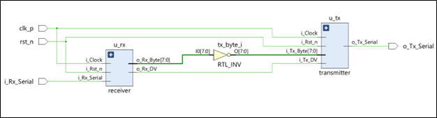
The top module computes this once and hands it to both blocks so TX and RX share the exact bit period. The clock comes straight from the board clock (held as a single‑ended net in this version), and reset is active‑low. On the serial side, the top module listens on the RX pin and immediately inverts the incoming byte and feeds it to the transmitter module.
Instantiating TX and RX modules of device 2 in the top module
The receiver and transmitter are instantiated side‑by‑side and driven by the same clock. The RX asserts a one‑cycle data‑valid pulse when a full byte is captured; that pulse doubles as the TX “start” signal so transmission begins the moment a byte is ready. The RX’s output byte flows through a lightweight transform stage (bitwise inversion for the blog demo) into the TX’s input.
The loopback example for self‑test
To verify end‑to‑end behavior without extra hardware, the top module runs a closed‑loop self‑test: bytes arriving on RX are immediately transformed and re‑emitted on TX. For this demo, we use a simple bitwise NOT operation as the transformation, since it makes the output easy to predict and verify. For example: • send 0xA5, expect ~0xA5 = 0x5A on TX • send 0x55, expect 0xAA, and so on. This provides a quick way to confirm that the design is correctly detecting frames and sending them back with accurate timing.
6. Verification: Testbench & Simulation
The simulation builds an environment around the top. A 100 MHz clock is generated; clocks‑per‑bit is derived from the chosen baud (e.g., 115200 → ~868 cycles/bit); reset is asserted and released cleanly. A byte‑framing task drives the RX line similar to standard UART implementations: idle high, a low start bit for one bit period, eight data bits LSB‑first, then a high stop bit. After each send, the testbench waits long enough for the TX path to finish and then checks results with a tiny scoreboard that compares the observed transmitted data to the expected transformed value (i.e., the bitwise inverse of what was sent). Counters track pass/fail, and the simulation prints a summary at the end. Because the receiver samples mid‑bit and uses a two‑flip‑flop synchronizer on the asynchronous RX input, the RX behaves robustly in sim: edges are recognized, data bits land in the right positions, and the one‑cycle data‑valid pulse cleanly triggers the TX.
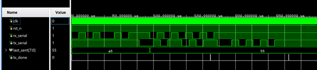
In the waveform above, the rx_serial line shows the UART receiver sampling two bytes back-to-back: first 0xA5 (1010 0101 in binary, sent LSB-first) and then 0x55 (0101 0101). You can clearly see the start bit (0), followed by the data bits, and finally the stop bit (1). The tx_serial line echoes the processed data. Since the design inverts each received byte (tx_byte = ~rx_byte), the transmitted patterns correspond to 0x5A and 0xAA instead.
7. On‑Board Testing & Validation
When we move off the simulator and onto a board, there are two straightforward ways to validate the design:
A) External USB‑UART dongle
The simplest way to test the design on hardware is by connecting it to a PC through a USB-UART adapter. Most FPGA boards expose header pins (such as PMOD connectors) that can be mapped to our UART’s TX and RX signals. By assigning these signals in the constraints file, we can physically route the FPGA’s TX and RX pins to the USB-UART dongle. On the PC side, a serial terminal program (like PuTTY/Tera Term) can be used to send and receive bytes. We set the terminal to the same UART settings as our design, that is, baud rate (e.g., 115200), 8 data bits, no parity, and 1 stop bit (8-N-1). Once connected, we can type a byte in the terminal and immediately see the board echo back the transformed value.
B) On-chip CPU driven self‑test .
The Zynq board has two main parts: a CPU, called the Processing System (PS), and the FPGA fabric, called the Programmable Logic (PL). This means the CPU can directly talk to our custom RTL design in the PL. One way to connect them is through EMIO (Extended Multiplexed I/O) which are basically a set of internal wires that route signals from the CPU into the FPGA fabric without going out through pins.
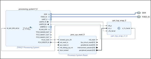
In our case, we used a UART peripheral on the CPU and route its TX and RX through EMIO into the PL, where they connect to the UART RTL. A bare-metal program running on the CPU then sends bytes into the PL’s RX and reads the results back from the PL’s TX. So, the CPU becomes a built-in testbench, making it easy to verify the design entirely on-board without any external adapters. Further details of this approach will be covered in the next post.