
Post 2: PS-PL Integration (Vivado Setup)
Published:
Written by Shreya Datir, in collaboration with Muhammad Farhan Azmine
Part 2: PS–PL Integration (Vivado Setup)
In the previous post, we designed a UART using FSMs, verified it in simulation, and looked at two ways to test it on hardware - an external USB–UART dongle and the PS–PL approach. While the external dongle method works, Zynq boards give us a more powerful option: using the Processing System (PS) as a built-in testbench for our RTL logic in the Programmable Logic (PL). The PS–PL integration is useful because:
- It removes the need for external adapters or cables.
- The CPU can send data directly into the UART RTL and read back results.
- We can write flexible bare-metal C programs for testing.
- It allows us to debug more easily by printing logs from the PS while interacting with our PL design.
This flow is not only convenient for on-board testing but also reflects how real Zynq projects combine software and hardware.
In this post, we’ll walk through the steps needed to set up PS–PL integration in Vivado:
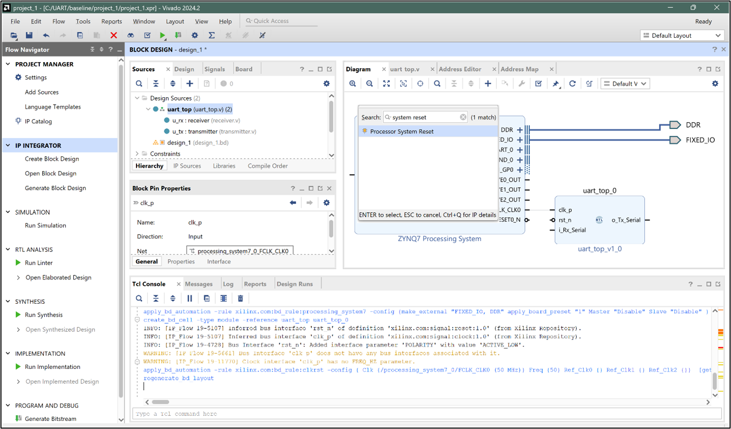
PS Configuration in Vivado
The first step is configuring the Zynq Processing System (PS) in Vivado. Inside the Zynq PS block, we can enable peripherals such as UART0 and UART1.
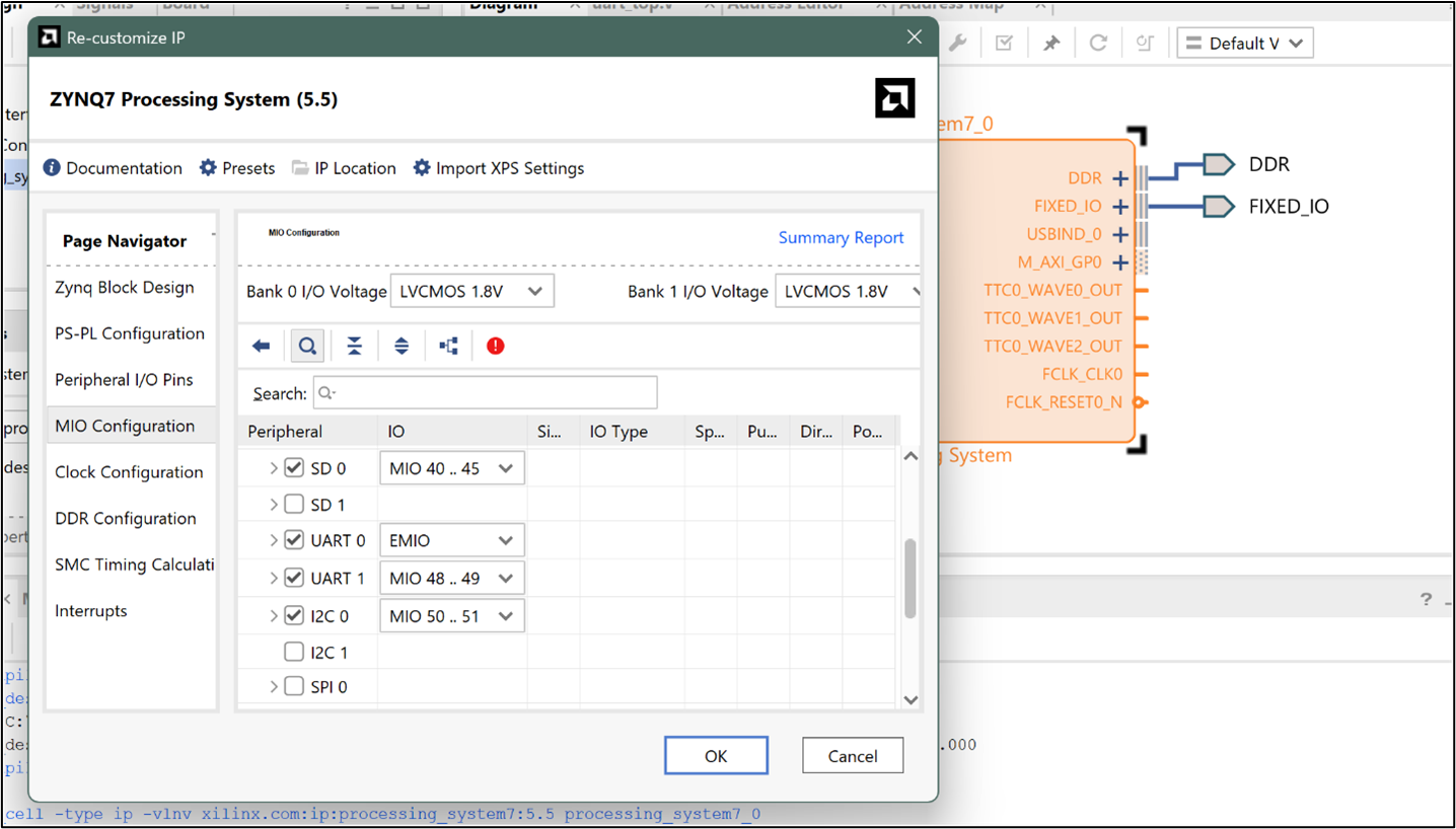
- MIO (Multiplexed I/O): maps a PS peripheral directly to physical package pins on the Zynq, e.g., to connect to a USB cable or external device.
- EMIO (Extended MIO): routes signals internally into the PL, so the custom RTL logic can use them.
For our setup:
- PS-UART1 is mapped via MIO so it can print to the console.
- PS-UART0 is routed via EMIO into the PL, where it connects to our UART RTL.
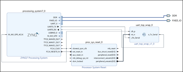
Vivado block diagram with PS UART0 → EMIO → PL and PS UART1 → MIO
Once this block diagram is complete, we export the hardware from Vivado, generating an .xsa file for use in Vitis.
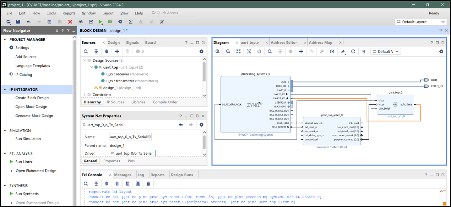
Overall Flow of PS–PL Integration
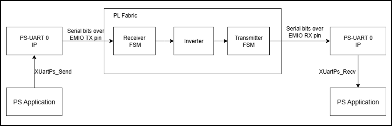
The setup works as shown in the diagram above.
- The PS Application running on the Zynq CPU uses PS-UART0, which is routed through EMIO into the PL fabric.
- Inside the PL, the data first passes through the Receiver FSM, which reconstructs bytes from the serial stream.
- The byte is then passed through a simple Inverter module (our demo transformation logic).
- The transformed data is serialized again by the Transmitter FSM and sent back through PS-UART0.
- Finally, the PS Application receives this processed data, where it can be checked and logged to the console.
Meanwhile, PS-UART1 (MIO) is used separately for console I/O, so all xil_printf() messages from the application are displayed on the PC terminal.
This flow lets the PS act as a built-in testbench: it generates test data, sends it through the PL UART RTL, and verifies the returned results.
Building the block diagram in Vivado
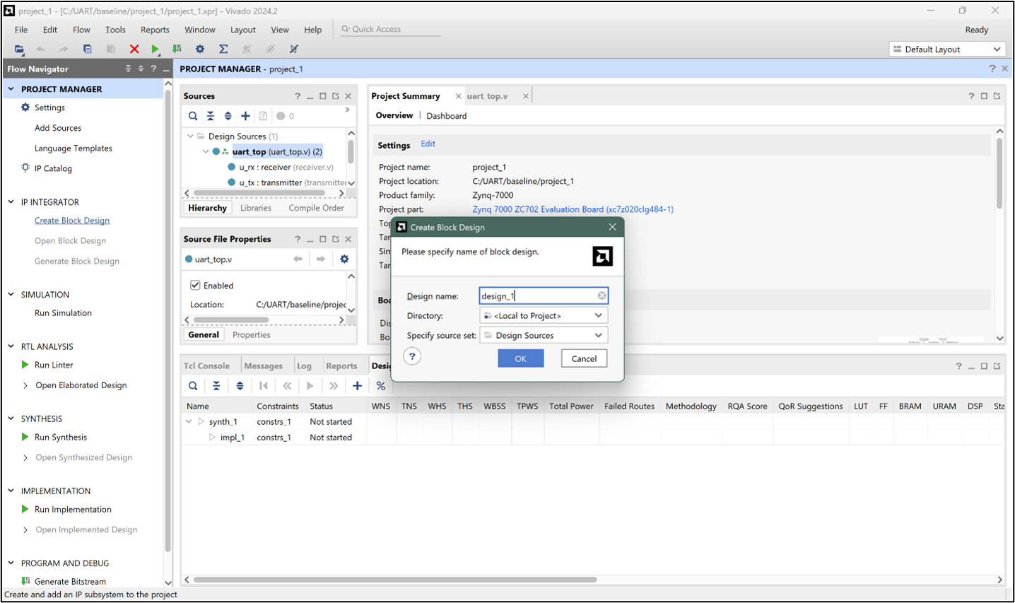
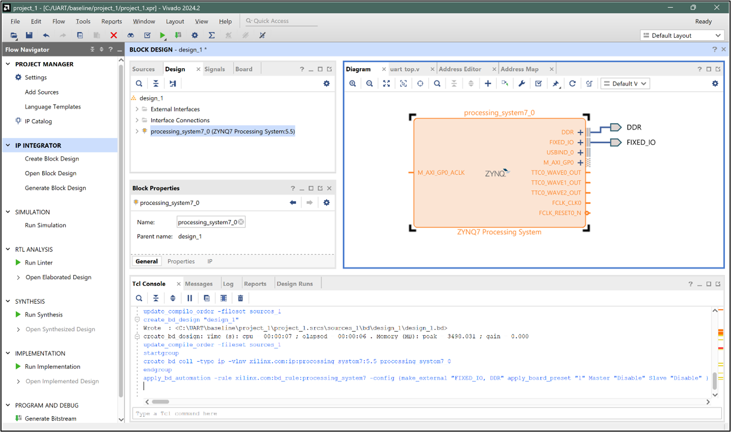
Step 1: Once the RTL design is ready and verified with a testbench, create a new Block Design from the Flow Navigator.
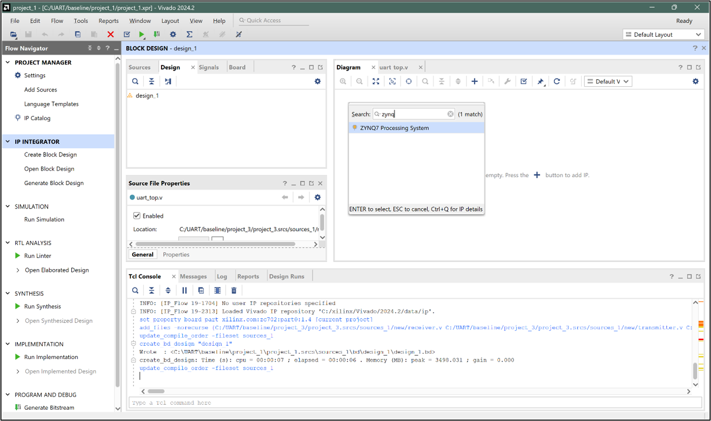
Step 2: Add the Zynq Processing System to the Block Diagram.
Step 3: Select the Zynq PS block and enable UART0 and UART1 from the Peripheral I/O Pins section.
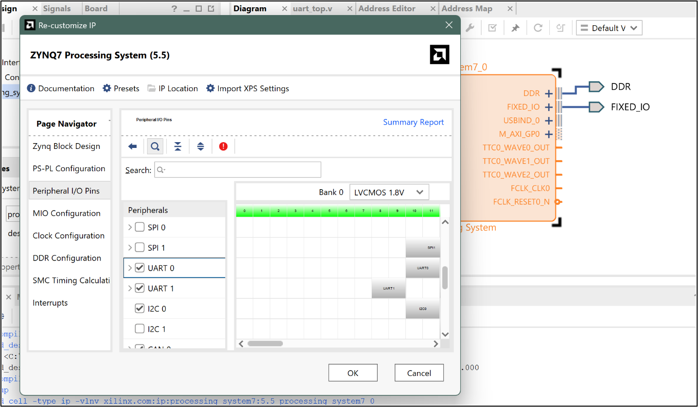
Step 4: Ensure that UART0 is set to EMIO and UART1 is set to MIO.
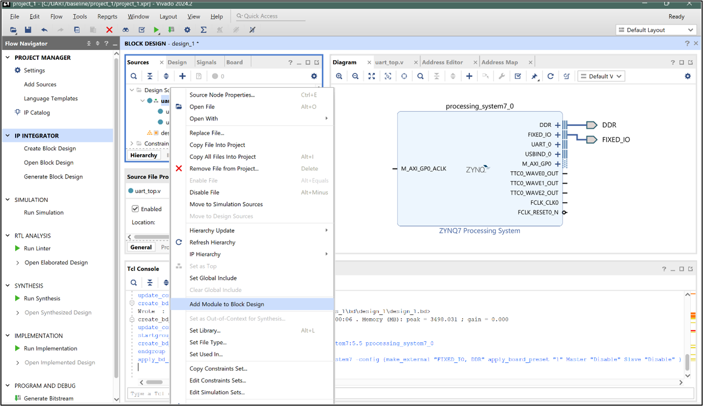
Step 5: In the Design Sources window, right-click on your top module and add it to the Block Design.
Step 6: Add a Processor System Reset block to the design. This block generates properly synchronized reset signals for the logic in the PL, ensuring that all modules start in a known state when the system powers up or resets.
Step 7: Connect the blocks together in the Block Design. Specifically:
- Connect the FCLK_CLK0 output from the Zynq PS to the clk input of your uart_top module and the Processor System Reset block.
- Connect the peripheral_aresetn output from the Processor System Reset block to the reset input of your uart_top module.
- Link the UART0 EMIO signals from the PS to the RX/TX ports of your uart_top.
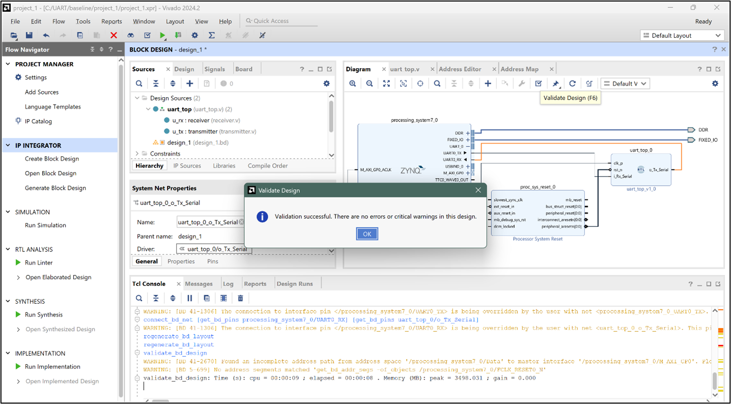
Step 8: Validate the design to ensure that all connections are correct and that there are no errors or missing links in the block diagram.
Step 9: In the Sources window, right-click on the block design and select Create HDL Wrapper to generate a top-level file for synthesis and implementation.
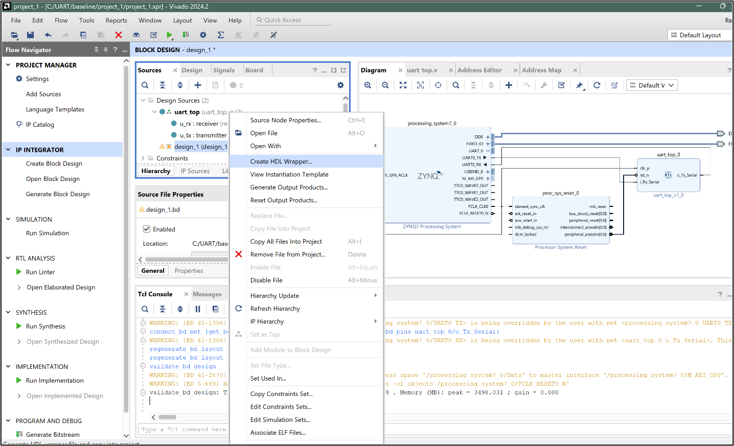
The HDL wrapper is a top-level entity required by design tools. It is necessary because the block design cannot be synthesized directly.
Step 10: Let Vivado manage wrapper and auto-update and click OK.
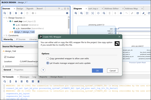
This will create a wrapper.v file and set it as the top module automatically.
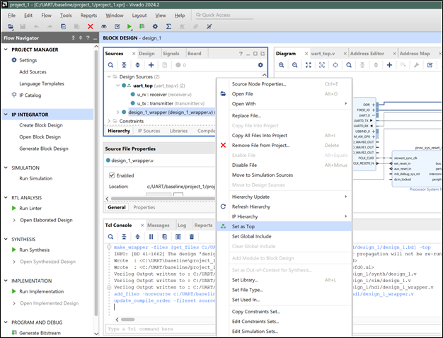
Step 11: The file design_wrapper.v is generated. Vivado usually sets this as the top automatically, but if not, you can right-click on it in the Sources window and select Set as Top manually.
Step 12: Generating the Block Design
- In the Flow Navigator window, click Generate Block Design under IP Integrator.
- Set the synthesis option to Global.
- Click Generate to build the required output products.
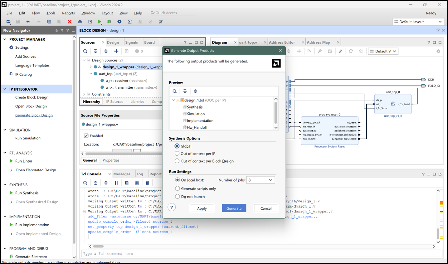
At this stage, Vivado automatically generates all the necessary files for the design. We don’t need to manually create constraints for the Zynq Processing System. Vivado generates an XDC file for it as part of this step.
Reference: AMD Zynq Embedded Design Tutorial
-Once the process is complete, click OK. 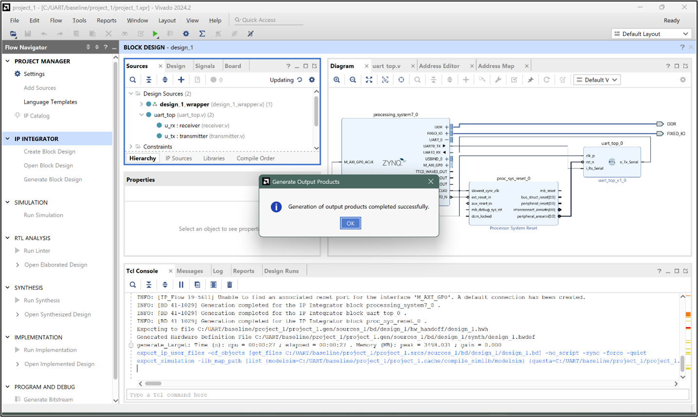
Step 13: Run Synthesis and Implementation in Vivado, and verify that both processes complete successfully without errors.
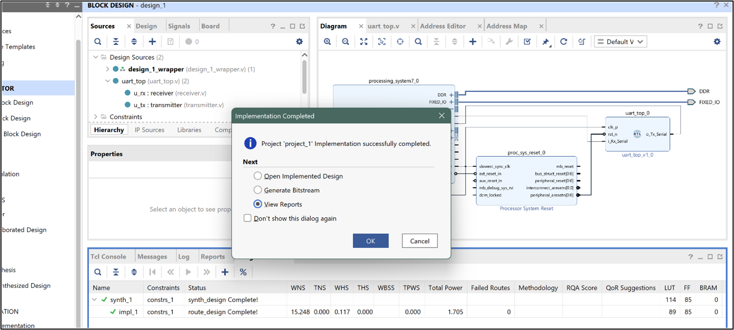
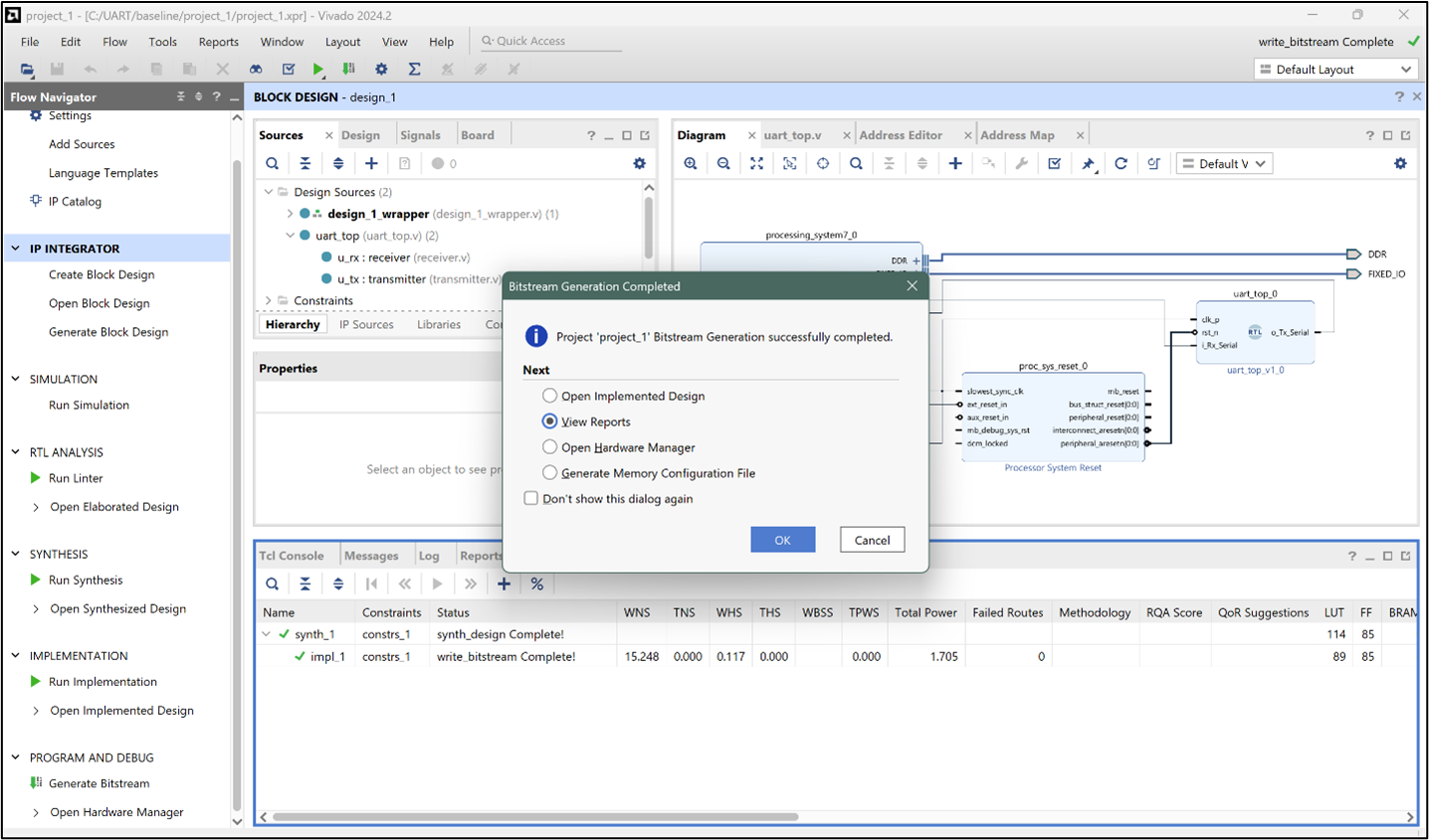
Step 14: From the Flow Navigator, click Generate Bitstream and confirm that the process completes successfully without errors.
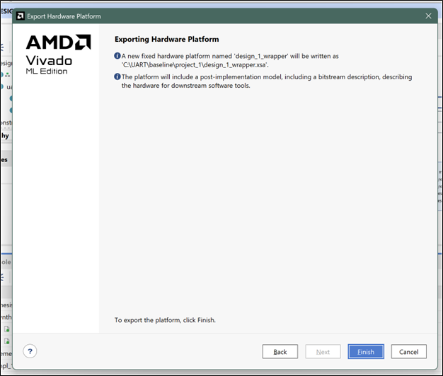
Step 15: Exporting the hardware.
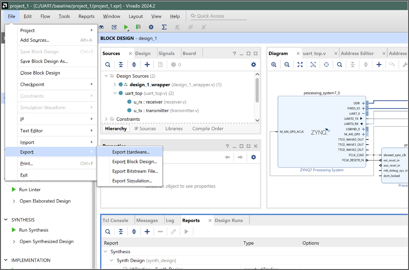
In the dialog box, make sure to check Include Bitstream so the hardware description contains both the design and the generated bitstream.
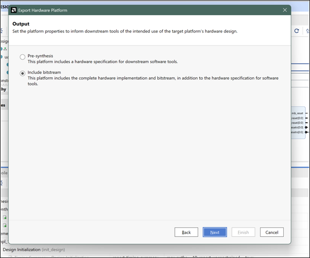
- Choose an output location (by default, Vivado will place it in your project’s folder).
- Click Finish to generate the .xsa file.
This .xsa (Xilinx Support Archive) file is what you’ll import into Vitis to create your software platform and bare-metal application.
Code & Resources
All source files, Vivado project (.xpr), and testbench code used in this post are available here:
UART-Communication-System GitHub Repository
You can download the full Vivado project as a zip and open it directly in Vivado (File → Open Project → select .xpr).
In the next part, we’ll take this exported hardware into Vitis, set up the BSP, and build a bare-metal application to test the UART design.